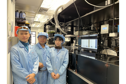
Experimental Condensed Matter and Material Science Group


AFM image, PL/ PLE spectra and theoretical results of self-assembled InGaAs QDs uncapped with GaAs layer


Transient setup and GaN:Co surface

People

Academic staff

Research staff

Students

Prof. Xiaodong CUI
Prof. Aleksandra B. DJURIŠIĆ
Prof. Dong-Keun KI
Prof. Francis C.C. LING
Prof. Mao Hai XIE


Dr. Ishaq AHMAD
Dr. Yicong CHEN
Dr. Tanmay MAITY
Dr. Hongbo MO
Dr. Qing RAO
Mr. Atta Ur REHMAN
Ms. Wenting SUN
Dr. Xiong WANG
Dr. Yipu XIA
Dr. Hongxia XUE
Dr. Mengfei YUAN
Dr. Junqiu ZHANG

Mr. Kai FENG (PhD)
Miss Yin LI (PhD)
Miss Zhiyue LI (PhD)
Mr. Tianxiang LIN (PhD)
Mr. Qiye LIU (PhD)
Mr. Zhilin REN (PhD)
Miss Xinyu WANG (PhD)
Mr. Yantao WANG (PhD)
Mr. Yueyang WANG (PhD)
Ms. Jing YU (PhD)
Mr. Tianyu ZHANG (PhD)
Mr. Yi ZHANG (PhD)
Mr. Yu ZHANG (PhD)


Research Activities

The group's research activities include electronics and optoelectronics of two-dimensional materials, organic/inorganic nanocomposite optoelectronic devices, epitaxial thin films and surface properties of new quantum materials, defects and nanostructures in semiconductors, and semiconductor optics.

Prof. Cui’s lab focuses on optical and electrical properties of nanostructures and emerging semiconductors. The laboratory is equipped with a home-made confocal spectroscopy system, a time-resolved spectroscopy system and an electric charactering system. Current research’s emphases include characterizations and applications of low dimensional materials, particularly emerging low dimensional semiconductors. Recently we focus on optical properties of atomic 2 dimensional (2D) crystals, particularly atomic layers of transition metal dichalcogenides (TMD).  We explore the interplay of electron’s spin, valley degrees of freedom and electron-electron interactions with semiconductor optics techniques.

Prof. Ki's quantum device lab investigates quantum transport phenomena in nano-electronic devices, realized by state-of-the-art nanofabrication and engineering techniques, such as electron-beam lithography and van der Waals assembly techniques. For this, the group is equipped with a complete set of nanofabrication and engineering facilities, such as electron-beam writer, mask-free photolithography system, metal deposition chambers, reactive ion etcher, and home-made micro-manipulators to assemble atomically thin 2D crystals with high precision. There are also two atomic force microscopes (AFMs) to check and clean 2D materials’ surfaces. For transport measurements, we have one zero-field 10K CCR cryostat, one 100 mK dilution fridge with 14-T magnet, one 400mK He-3 fridge with 12-T magnet, and one 1.8K 9-T PPMS. Current research focuses on discovering new transport phenomena, understanding their microscopic origins, and learning to control their properties. Materials of interest include 2D materials, topological insulators, unconventional magnets, and low-dimensional Perovskite nanostructures as they not only have interesting electronic properties but also offer large experimental flexibilities to study and engineer them. We are also interested in bridging the gap between the fundamental research and real-life applications. 

More details can be found at http://www.physics.hku.hk/~dkkilab/

Prof. Djurišić’s research activities include fabrication and characterization of organic/inorganic halide perovskite optoelectronic devices (light emitting diodes and solar cells), as well as fabrication and characterization of wide band gap semiconductor nanostructures, primarily for application as charge transport materials in optoelectronic devices. The study of optoelectronic devices aims at improving the understanding of the operating principles and processes taking place at interfaces. The obtained results are then used for fabrication of devices with improved performance, with particular emphasis on device stability. This research also includes the investigation of novel halide materials, and understanding the relationship between their chemical composition and their optical and electronic properties. The laboratory is equipped with fume cupboards, glove box, tube furnaces, spin-coater, two thermal evaporators for fabrication of optoelectronic devices, and E-beam/sputtering deposition system, while characterization facilities include UV/Vis/NIR spectrometers for characterization of light emitting diodes and experimental setups for power conversion efficiency and external quantum efficiency measurements for solar cells.

Prof. Ling’s current focused interests of the Material Physics Laboratory include:
(1) Defects in semiconductors: characterizations and identifications, defects influence on materials electrical, optical and magnetic properties, defect control, defects at semiconductor junctions;
(2) Electrical and optical properties of semiconductor system: deep level transient spectroscopy, temperature dependent Hall measurement, IV and CV measurements, luminescence spectroscopy;
(3) Positron annihilation spectroscopic study of vacancy type defects: These research activities are performed with the positron beam line located at the electron LINAC ELBE, Helmoltz Zentrum Dresden Rossendorf, Germany.
(4) Defects in functional oxides and wide band-gap materials: Tailoring electrical, optoelectronic, dielectric and magnetic properties of these materials and devices via defect engineering.

The lab is equipped with specialised equipment such as Laplace transformed deep level transient spectroscopy system; Liquid nitrogen optical cryostat; 10 K liquid He free optical cryostat; Electrical characterization equipment: semiconductor parameter analyzer, multi-frequency LCR meter, pico- ammeter, electrometer, and etc.; Photoluminescence system: 30 mW HeCd laser, 500 mm monochrometer, PMT and CCD detecting system; UV-visible spectrophotometer; Radio frequency magnetron sputtering system; Pulsed laser deposition system; Chemical vapor deposition system; Electron beam evaporator; Thermal evaporator; Tube furnace and box furnace. Big “off campus” equipment accessible to our students and staff: Positron beam time at the electron LINAC ELBE in the Center for High-Power Radiation Sources, Helmoltz Zentrum Dresden Rossendorf (HZDR), Germany for positron annihilation spectroscopic (PAS) study.

Prof. Xie’s research aims at understanding the processes and properties that occur at the boundary of materials surface. Current researches focus on the growth and surface characterizations of low-dimensional materials, such as transition-metal dichalcogenides and their hetero-structures. We use molecular-beam epitaxy (MBE), one of the most versatile techniques to grow materials with precise control, to fabricate new quantum materials and artificial structures with single atomic layer precision. We characterize the structural and electronic properties by surface tools such as scanning tunneling microscopy and spectroscopy (STM/S) and ultraviolet photoelectron spectroscopy (UPS). 

Some Representative Publications

(For the complete publication list of the department, please go back to Research.)


Prof. X.D. Cui

  1. "Manipulating spin-polarized photocurrents in 2D transition metal dichalcogenides", L. Xie, X. Cui, Proceedings of the National Academy of Sciences, 113, 14, 3746-3750 (2016)
  2. “Anomalously robust valley polarization and valley coherence in bilayer WS2”, B. Zhu, H.L.Zeng, J.F. Dai, Z.R. Gong and X.D. Cui, Proceedings of the National Academy of Sciences of the United States of America (PNAS), 111, 11606-11611 (2014) 
  3. "Optical signature of symmetry variations and spin-valley coupling in atomically thin tungsten dichalcogenides", H. Zeng, G.B. Liu, J. Dai, Y. Yan, B. Zhu, R. He, L. Xie, S. Xu, X. Chen, W. Yao and X.D. Cui, Scientific Reports, 3, 1068 (2013) 
  4. "Valley polarization in MoS2 monolayers by optical pumping", H.L. Zeng, J.F. Dai, W. Yao, D. Xiao and X.D. Cui, Nature Nanotechnology, 7, 490-493 (2012) 
  5. “Magnetoelectric Photocurrent Generated by Direct Interband Transitions in InGaAs/InAlAs Two-Dimensional Electron Gas”, J.F. Dai, H.F. Lu, C.L. Yang, S.Q. Shen, F.C. Zhang and X.D. Cui; Physical Review Letters, 104, 246601 (2010) 
  6. “Observation of exciton-phonon sideband in individual metallic single-walled carbon nanotubes”, H.L. Zeng, H.B. Zhao, F.C. Zhang and X.D. Cui, Physical Review Letters, 102, 136406 (2009) 


Prof. A.B. Djurišić

  1. “Cesium Doped NiOx as an Efficient Hole Extraction Layer for Inverted Planar Perovskite Solar Cells”, W. Chen, F.Z. Liu, X.Y. Feng, A.B. Djurišić, W.K. Chan, Z.B. He, Advanced Energy Materials, 1700722 (2017) 
  2. “Is excess PbI2 beneficial for perovskite solar cell performance?”, F. Z. Liu, Q. Dong, M. K. Wong, A. B. Djurišić, A. Ng, Z. W. Ren, Q. Shen, C. Surya, W. K. Chan, J. Wang, A. M. C. Ng, C. Z. Liao, H. K. Li, K. M. Shih, C. R. Wei, H. M. Su, and J. F. Dai, Advanced Energy Materials, 6, 1502206 (2016)
  3. “Hydrothermally synthesized CuxO as a catalyst for CO oxidation”, M.Y. Guo, F.Z. Liu, J.K. Tsui, A.A. Voskanyan, A.M.C. Ng, A.B. Djurišić, W.K. Chan, K.Y. Chan, C.Z. Liao, K.M. Shih and C. Surya, Journal of Materials Chemistry A, 3, 3627-3632 (2015)
  4. “Mechanisms of Antibacterial Activity of MgO: Non-ROS Mediated Toxicity of MgO Nanoparticles Towards Escherichia coli”, Y.H. Leung, A.M.C. Ng, X.Y. Xu, Z.Y. Shen, L.A. Gethings, M.T. Wong, C.M.N. Chan, M.Y. Guo, Y.H. Ng, A.B. Djurišić, P.K.H. Lee, W.K. Chan, L.H. Yu, D.L. Phillips, A.P.Y. Ma and F.C.C. Leung, Small, 10, 1171-1183 (2014)
  5. “In situ synthesis of CuxO/SnOx/CNT and CuxO/SnOx/SnO2/CNT nanocomposite anodes for lithium ion batteries by a simple chemical treatment process”, X. Liu, F. Z. Liu, Q. Sun, A. M. C. Ng, A. B. Djurišić, M. H. Xie, C. Z. Liao, K. M. Shih,ACS Appl. Mater. & Interfaces , 6, 13478-13486 (2014)


Prof. D.K. Ki

  1. “A family of finite-temperature electronic phase transitions in graphene multilayers", Y. Nam, D.K. Ki, D. Soler-Delgado, and A.F. Morpurgo, Science, 362, 324 (2018)


Prof. F.C.C. Ling

  1. “Thermal evolution of defects in undoped zinc oxide grown by pulsed laser deposition”, Zilan Wang, Shichen Su, Francis Chi-Chung Ling, W. Anwand, and A. Wagner, J. Appl. Phys., 116, 033508 (2014)
  2. “Impedance analysis of secondary phases in a Co-implanted ZnO single crystal”, M. Younas, L. L. Zou, M. Nadeem, Naeem-ur-Rehman, S. C. Su, Z. L. Wang, W. Anwand, A. Wagner, J. H. Hao, C. W. Leung, R. Lortz, and F. C. C. Ling, Phys. Chem. Chem. Phys., 16, 16030 (2014)
  3. “Low-threshold lasing action in an asymmetric double ZnO/ZnMgO quantum well structure”, S.C. Su, H. Zhu, L.X. Zhang, M. He, L.Z. Zhao, S.F. Yu, J.N. Wang and F. C.C. Ling, Appl. Phys. Lett., 103, 131104 (2013)
  4. “Current transport studies of ZnO/p-Si heterostructures grown by plasma immersion ion implantation and deposition”, X. D. Chen, C. C. Ling, S. Fung, C. D. Beling, Y. F. Mei, Ricky K. Y. Fu, G. G. Siu, Paul K. Chu,Appl. Phys. Lett., 88, 132104 (2006)
  5. “Low energy electron irradiation induced deep level defects in 6H-SiC: The implication for the microstructure of the deep levels E1/E2”, X.D. Chen, C.L. Yang, M. Gong, W.K. Ge, S. Fung, C.D. Beling, J.N. Wang, M.K. Lui and C.C. LingPhys. Rev. Lett., 92, 125504 (2004)


Prof. M.H. Xie

  1. "Hole doping in epitaxial MoSe2 monolayer by nitrogen plasma treatment”, Yipu Xia, Bo Wang, Junqiu Zhang, Yue Feng, Bin Li, Xibiao Ren, Hao Tian, Jinpeng Xu, Wingkin Ho, Hu Xu, Chang Liu, Chuanhong Jin, and Maohai Xie, 2D Mater. 5, 041005 (2018)
  2. "One-dimensional phosphorus chain and two-dimensional blue phosphorene grown on Au (111) by molecular-beam epitaxy", J.P. Xu, J.Q. Zhang, H. Tian, H. Xu, W.K. Ho, M.H. Xie. Phys. Rev. Mater., 1, 061002(R)(2017)
  3. "Inversion Domain Boundary Induced Stacking and Bandstructure Diversity in Bilayer MoSe2", J.H. Hong, C. Wang, H.J. Liu, X.B. Ren, J.L. Chen, G. Wang, J.F. Jia, M.H. Xie, C.H. Jin, W. Ji, J. Yuan, Z. Zhang, Nano Letter, 17, 11, 6653-6660 (2017)
  4. "Quantum effects and phase tuning in epitaxial hexagonal and monoclinic MoTe2 monolayers”, J. Chen, G.Y. Wang, Y.A. Tang, H. Tian, J. Xu, X.Q. Dai, H. Xu, J.F. Jia, W.K. Ho, M.H. Xie, ACS Nano, 11, 3282 (2017)
  5. “Observation of intervalley quantum interference in epitaxial monolayer tungsten diselenide”, H.J. Liu, J.L. Chen, H.Y. Yu, F. Yang, L. Jiao, G.B. Liu, W.K. Ho, C.L. Gao, J.F. Jia, W. Yao, M.H. XieNat. Comm., 6, 8180 (2015)
  6. “Line and point defects in MoSe2 bilayer studied by scanning tunneling microscopy and spectroscopy”, H.J. Liu, H. Zheng, F. Yang, L. Jiao, J.L. Chen, W.K. Ho, C.L. Gao, J.F. Jia, M.H. Xie, ACS Nano., 9, 6619 (2015)
  7. “Molecular-beam epitaxy of monolayer and bilayer WSe2: a scanning tunneling microscopy / spectroscopy study and deduction of exciton binding energy”, H.J. Liu, L. Jiao, L. Xie, F. Yang, J.L. Chen, W.K. Ho, C.L. Gao, J.F. Jia, X.D. Cui, M.H. Xie, 2D Mater.2, 034004 (2015)
  8. “Dense network of one-dimensional midgap metallic modes in monolayer MoSe2 and their spatial undulations”, H.J. Liu, L. Jiao, F. Yang, Y. Cai, X. Wu, W.K. Ho, C.L. Gao, J.F. Jia, N. Wang, H. Fan, W. Yao, M.H. Xie, Phys. Rev. Lett., 113, 066105 (2014)
Last updated on 01 March 2024