


RESEARCH AREAS


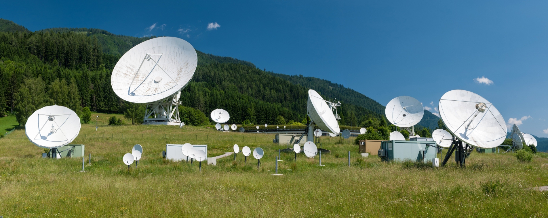
Astronomy and Astrophysics Group


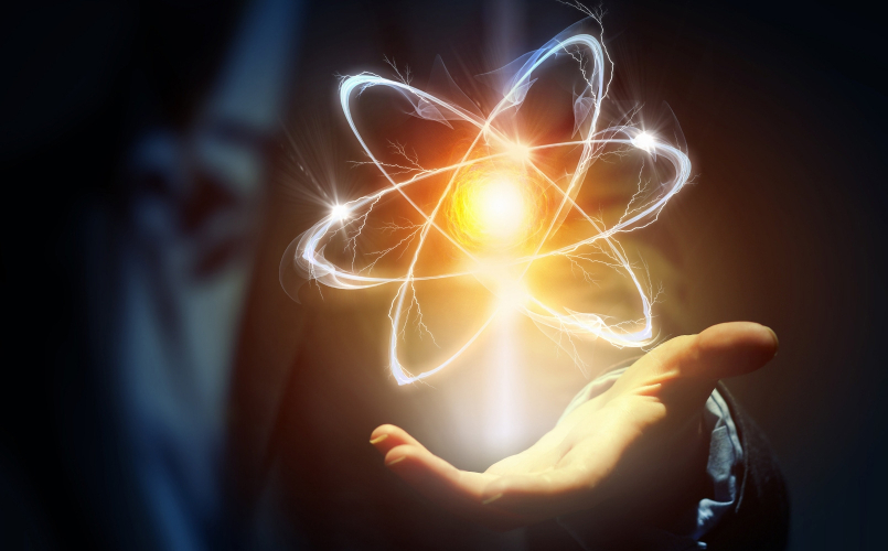
Atomic, Optical and Quantum Physics Group


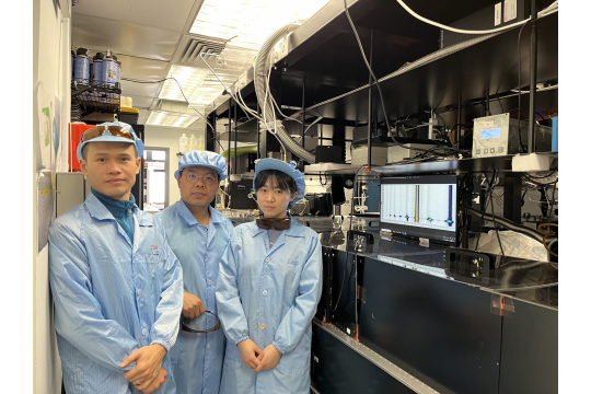
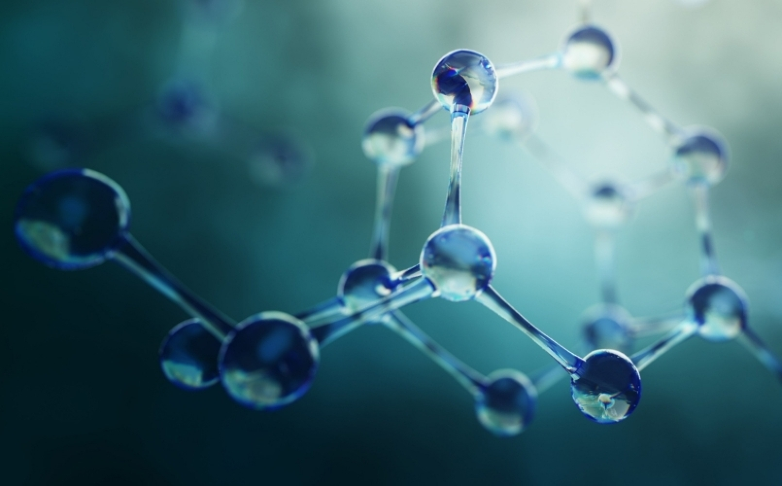
Experimental Condensed Matter and Material Science Group


Theoretical and Computational Condensed Matter Group


Experimental Nuclear and Particle Physics Group
In addition, the department also hosts one Area of Excellence Project – 2D Materials Research: Fundamentals Towards Emerging Technologies.


ABOUT US Learn More
The department is committed to excellence in teaching and research. It runs the major undergraduate programs of Physics, or minor of Physics and Astronomy and contribute to teaching of some other interdisciplinary programs, such as Environmental Science. It offers a number of postgraduate projects.